1. AML Hardware Toolkit
1.1. Introduction
Modern computing predominantly relies on general-purpose processors like CPUs because of their flexibility and ease of programming. However, this convenience comes with a significant energy cost and low throughput, as CPUs consume much more power and time for fetching and decoding instructions than performing basic operations. To address the need for both higher performance and energy efficiency, domain-specific accelerators, such as FPGAs and ASICs, offer a compelling alternative. These accelerators are tailored to specific computational tasks, making them far more efficient for workloads. While CPUs and GPUs are flexible and capable of handling a wide range of tasks, they struggle with irregular parallelism and limited precision support. In contrast, FPGAs can be reprogrammed for different tasks, and ASICs offer efficiency, though at the cost of flexibility and development complexity. In the ALMA project, the RPTU team was responsible for designing and developing a hardware accelerator specifically for Algebraic Machine Learning (AML). Existing hardware platforms, such as GPUs, are primarily optimized for AI applications, which have substantially different computational characteristics compared to AML. The compute demand of AML requires a platform specifically optimized for this algorithm. Our task was to design a hardware architecture that efficiently accelerates AML tasks.
1.2. Overview of Hardware Architecture
The proposed hardware architecture is a Single Instruction, Multiple Data (SIMD) processor designed to utilize parallel compute units for accelerating AML tasks. This parallelism makes them highly effective for tasks that involve large amounts of data that can be processed in parallel. The architecture groups multiple data into vectors, allowing one instruction to perform the same operation across all elements, thereby improving efficiency and reducing the overhead associated with repetitive instruction fetches. Although SIMD processors excel at tasks with regular, parallel data structures, they are less suited for irregular computations, which limits their flexibility in certain applications. Despite this, their ability to enhance performance and energy efficiency for specific workloads makes them a critical component in modern computing architectures. This architecture features numerous parallel cores as shown in Fig.1, each with its own memory hierarchy. Given that AML is a highly memory-bound application, we have incorporated High Bandwidth Memory (HBM) DRAM into our design. HBM is an advanced type of memory designed to provide significantly higher data transfer rates than traditional memory technologies, such as DDR (Double Data Rate) or GDDR (Graphics Double Data Rate). HBM achieves this by stacking multiple memory dies vertically, connected through TSVs (Through-Silicon Vias), and placing them in close proximity to the processor. This three-dimensional architecture minimizes the distance that data needs to travel, reducing latency and power consumption while greatly increasing bandwidth. HBM is particularly effective in applications that require massive data throughput, such as AML workloads. Its architecture allows for multiple parallel data paths, enabling data transfers at rates exceeding hundreds of gigabytes per second.
1.2.1. Key Features
- Parallel Cores and Memory Hierarchy:
The hardware architecture consists of parallel cores, each capable of independently computing an AML task.
Each core consists of computing units specifically designed for AML tasks. These units are internally parallelized, providing high throughput.
Each core is connected to a channel of HBM memory, enabling independent operation from other cores with high memory bandwidth.
Cores contain local scratchpad buffers, allowing data reuse and prefetching to minimize off-chip memory access.
- Custom Instruction Set:
The core operations are controlled through an in-house defined instruction set.
This instruction set includes details about the type of operation, size, and address of data, which the control unit uses to fetch data and activate the corresponding compute unit.
- PCIe Interface:
The architecture is equipped with a PCIe interface, making it compatible with any existing computing platform.
Users can offload time-consuming AML tasks to the hardware accelerator, leveraging parallelization to improve throughput.
Results from each task can be accessed through the PCIe interface.
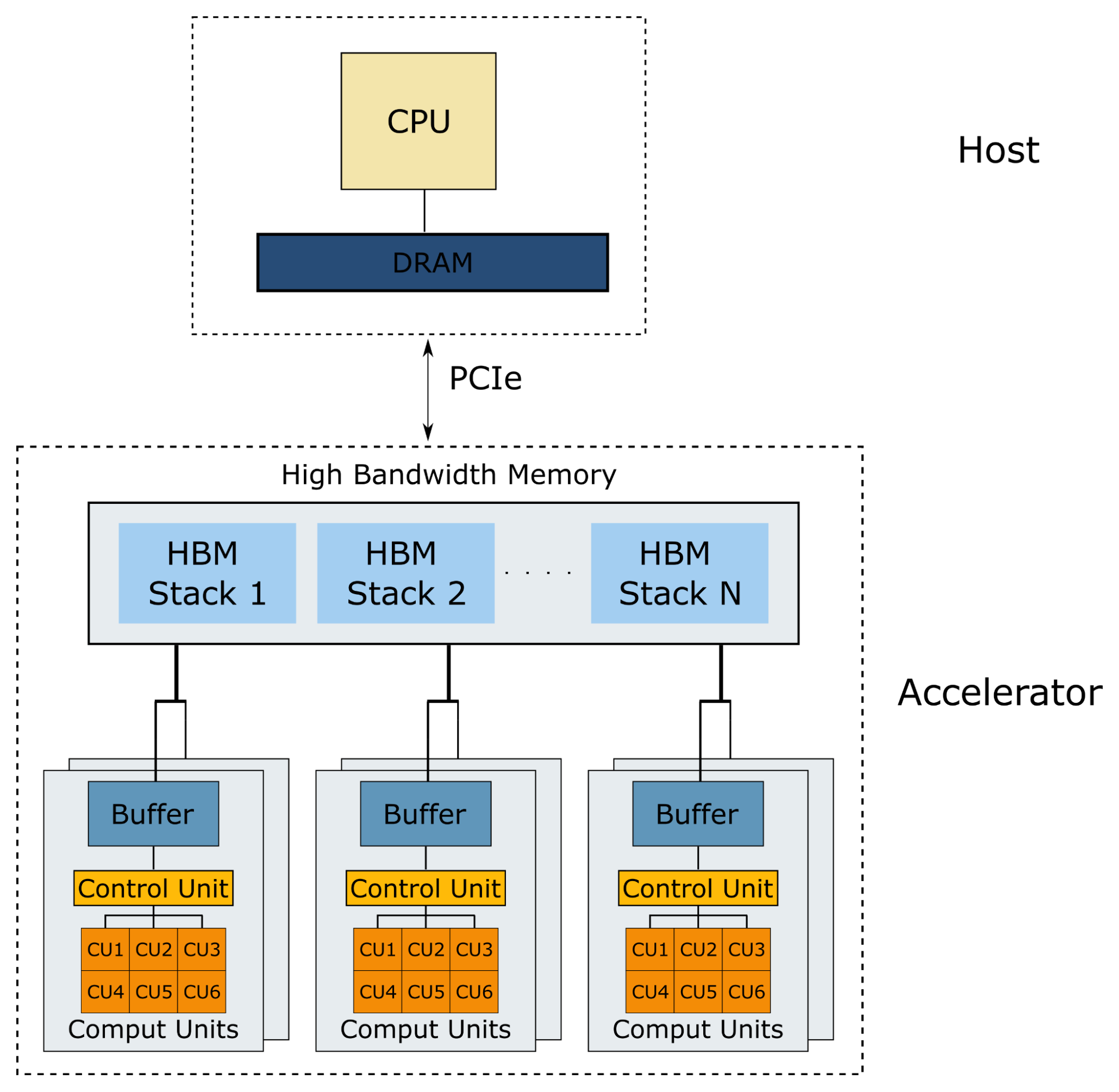
Fig. 1.1 Overview of AML Hardware Architecture.